
PVD APPLICATIONS

PVD Solutions for Advanced Metallization

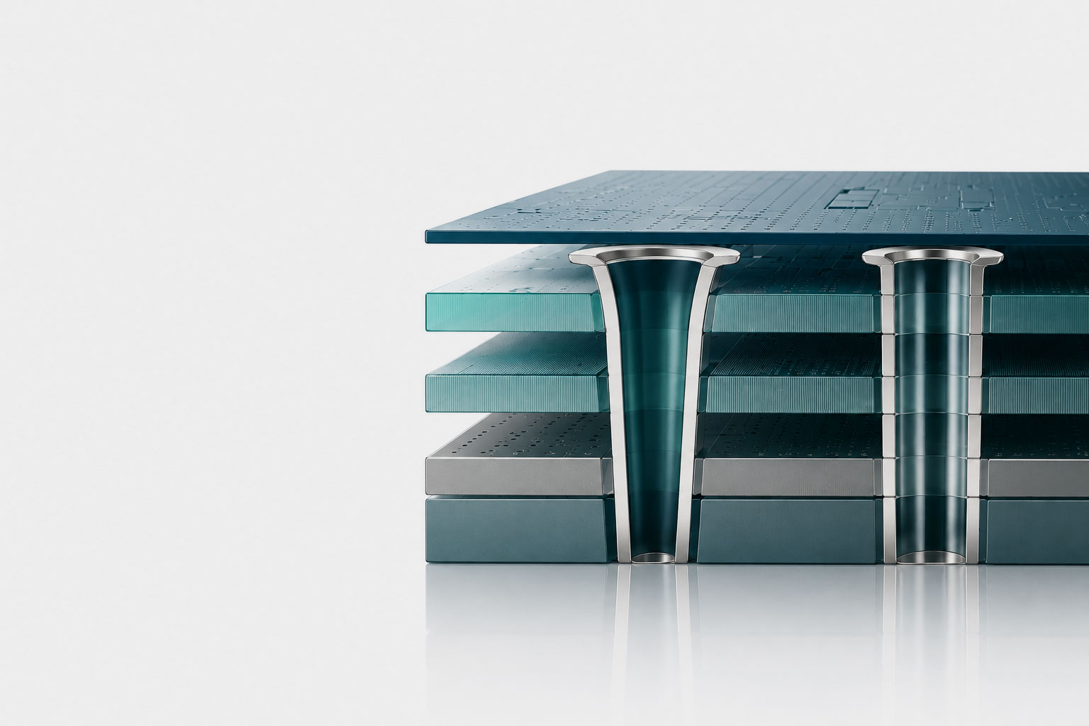
Cross-section diagram of a high aspect ratio through-glass via coating
01 — Semiconductor

Advanced 3D Packaging

FOPLP / TGV / TSV

High-aspect-ratio (HAR) TSV and TGV structures present critical deposition challenges: conventional sputtering often fails to achieve uniform sidewall and via-bottom coverage without voiding.
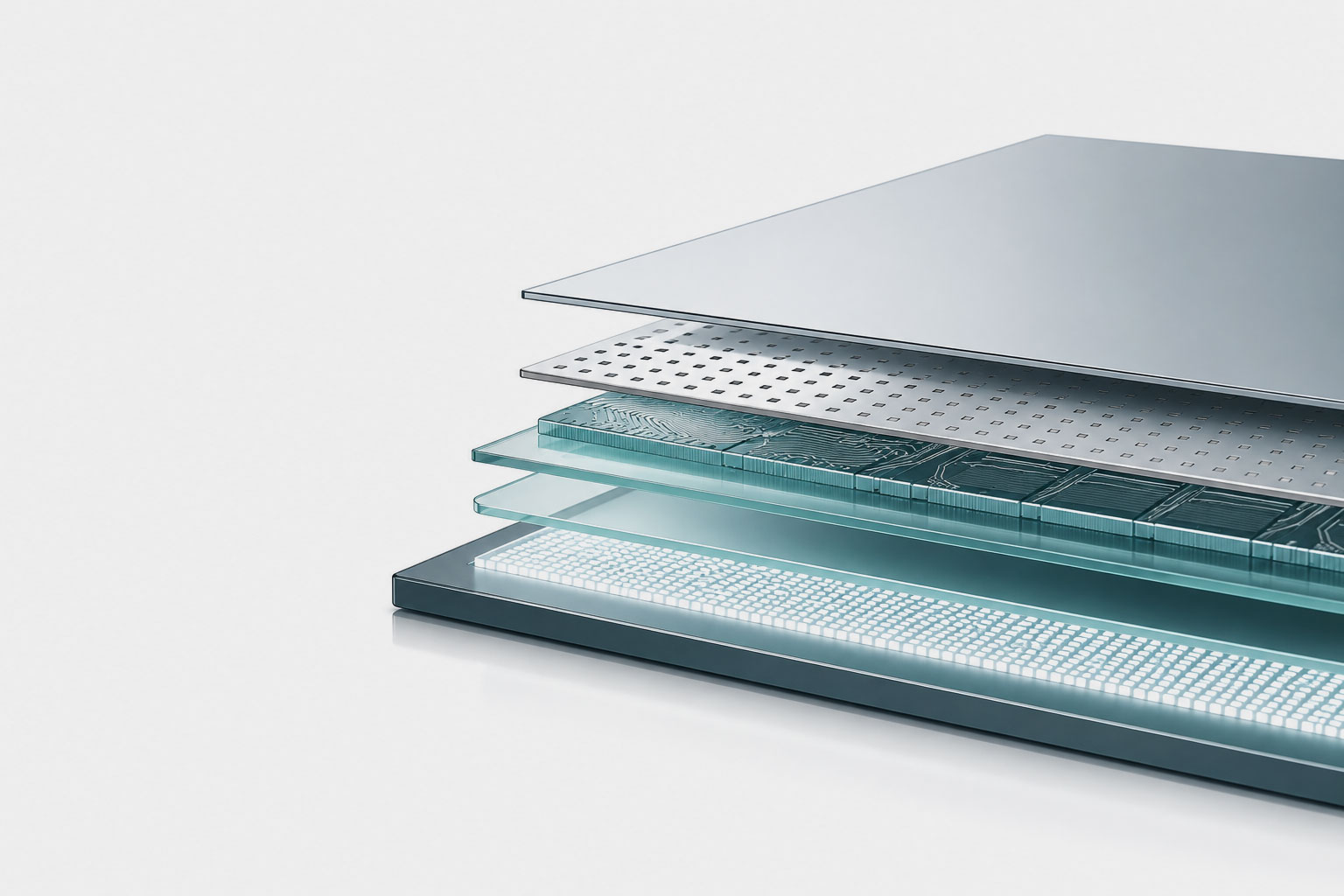
Advanced packaging seed layerFOPLP panel-level packagingTGV glass-via sputteringHigh aspect ratio (HAR) coatingStress controlUBMTi/Cu seed layer
CRITICAL PAIN POINTS
Coverage loss in high-aspect-ratio vias
As TSV and TGV aspect ratios climb, conventional sputtering can show neutral-particle scattering, leading to thin or discontinuous sidewall coverage and voiding during subsequent copper electroplating.
Substrate warpage from thick-metal film stress
Depositing thick copper or UBM on panel-level substrates (510×515mm) introduces film stress that can warp the panel, complicating automated handling and exposure alignment.
Adhesion loss at the metal-substrate interface
Smooth glass and low-surface-energy PI surfaces are difficult substrates for metal seed layers to bond to, which can lead to delamination during thick copper electroplating.
PVD SOLUTIONS
High-ionization, RF bias-guided deposition
High-density plasma with RF bias focusing improves sidewall and via-bottom step coverage, supporting TGV structures with aspect ratios up to 15:1.
Multi-zone thermal compensation and stress control
Process temperature is maintained below 150°C, with bias and pressure tuning designed to hold large-substrate warpage within 0.5mm.
CCP pre-clean and titanium adhesion layer
Integrated CCP Pre-Clean (SiO₂ etch uniformity ≤10%) with an engineered Ti adhesion layer achieves 5B cross-hatch adhesion and a high peel strength of 20 N/cm on PI—far exceeding the 1.0 N/mm industry baseline.
Smartphone display showing an under-screen fingerprint sensor illustration
02 — Display

Micro LED / Silicon Photonics / OLED

Panel-level metallization

Thick, low-resistance electrode layers at display scale place specific demands on deposition throughput and large-area uniformity.
Display metal electrodesMicro LED conductive layerOLED transparent conductive filmITO sputteringLow-resistance metal linesLarge-area uniformityPanel-level PVD
CRITICAL PAIN POINTS
Throughput limits on thick conductive layers
Display electrodes (Al, Cu, Mo) often require hundreds of nanometers of low-resistance metal. ALD may not provide the throughput required for thick conductive layers at production scale.
Sheet-resistance uniformity at large substrate sizes
At Gen 4.5 and Gen 6 substrate sizes, magnetron sputtering can be sensitive to edge effects and gas-flow variation, which affects Rs uniformity and, in turn, panel brightness and color consistency.
Thermal sensitivity of emissive materials
Quantum dot and OLED materials are sensitive to process temperature. Elevated deposition temperatures can reduce emissive lifetime and external quantum efficiency (EQE).
PVD SOLUTIONS
Large-area planar cathode PVD for higher UPH
The cathode design is built for thick conductive layers, with RDL throughput of ≥30 panels/hour (equivalent to roughly 111 twelve-inch wafers/hour).
Demonstrated large-area sheet-resistance uniformity
On 510×515mm substrates, measured Rs uniformity of approximately 3.05% for Ti film and 2.36% for Cu film.
Low-temperature, controlled ion-bombardment process
The vacuum process is tuned to limit thermal load and ion-induced surface damage, supporting temperature-sensitive display material stacks.
High density plasma source glowing blue inside a vacuum chamber viewport
03 — Precision Coating

MEMS & RF Devices

Piezoelectric films, sensors, bond pads

5G filters, acoustic sensors, and MRAM devices depend on film-level control that standard sputtering processes can struggle to hold consistently.
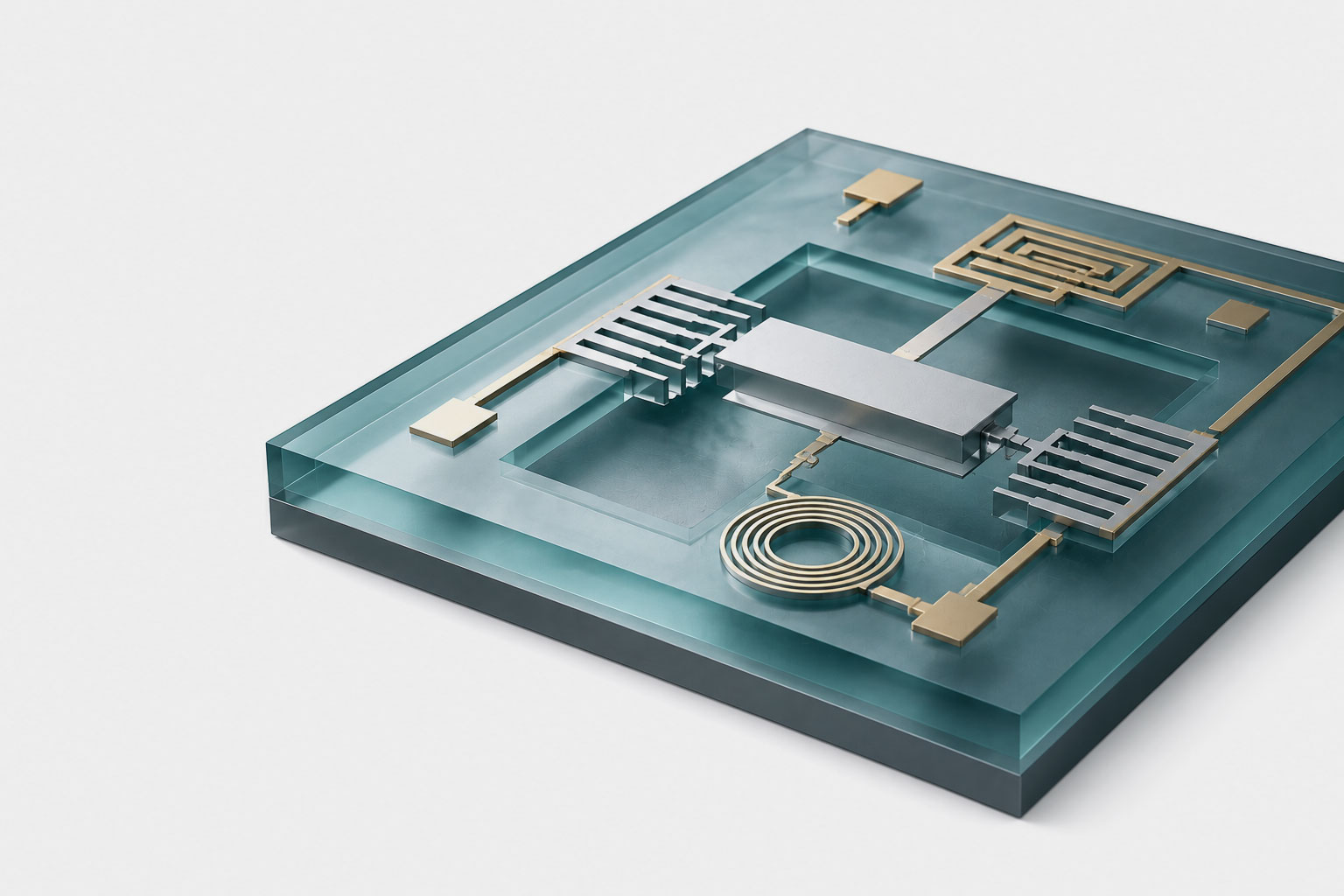
MEMS metal electrodesPiezoelectric film sputteringAlN aluminum nitrideMEMS PVDDLC diamond-like coatingWire-bond pad coating
CRITICAL PAIN POINTS
Crystal orientation control
5G RF filters and acoustic sensors (BAW/SAW) rely on piezoelectric film quality, such as AlN c-axis orientation. Deviation from the target orientation can reduce piezoelectric response and cause frequency drift.
Compositional control in multi-element alloys
Magnetic sensors and MRAM require precise nanoscale stacking of ferromagnetic alloys (NiFe, CoFeB). Standard sputtering can be prone to compositional drift across these multi-element films.
Bond pad durability under wire-bonding load
Sensor bond pads need sufficient thickness and adhesion to withstand wire-bonding impact during back-end packaging.
PVD SOLUTIONS
Directional reactive magnetron sputtering
RF plasma power and gas feedback control are tuned to promote oriented film growth, supporting piezoelectric films with a controlled c-axis lattice.
Multi-chamber cluster architecture
A fully vacuum, multi-chamber cluster design supports repeatable multi-element alloy composition with minimal cross-contamination between layer interfaces.
CCP pre-clean with high-utilization target
Front-end CCP pre-clean combined with a high-utilization planar target (40–50%) is used to deposit bond pad metallization validated against packaging pull-test requirements.
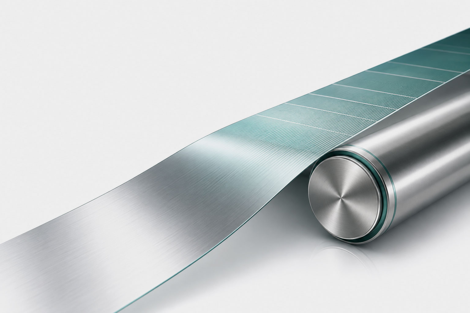
Roll-to-roll in-line PVD system for photovoltaic film production
04 — Green Energy

Lithium Battery & Solar

Roll-to-roll & panel-level metallization

Metallizing solar and battery substrates at scale places sustained demands on target utilization and thermal control.
Solar back-electrode sputteringLithium battery current collectorRoll-to-roll PVDPerovskite back-metal layerLow contact resistanceHigh target utilization
CRITICAL PAIN POINTS
Target utilization and cost of ownership
Solar back electrodes and battery current collectors require copper/aluminum foil metallization across large substrate areas. Conventional planar targets typically utilize under 30%, increasing PM frequency and replacement cost.
Thermal sensitivity of thin flexible substrates
Thin battery substrates and perovskite films are sensitive to process temperature; above roughly 180°C, flexible foils can deform and perovskite structures can degrade.
Wastewater considerations with wet electroplating
Wet electroplating processes generate heavy-metal-containing wastewater, which adds handling and compliance requirements under tightening environmental standards.
PVD SOLUTIONS
High target utilization and extended lifetime
A large-area planar cathode design achieves target utilization above 50%, with Ti target life up to 15,000 kWh and Cu target life up to 5,000 kWh, and PM changeover typically under 2 hours.
Thermal-gradient transport control (under 150°C)
A transport and ramp system for heat-sensitive, thin substrates maintains deposition rate while keeping the process environment within a controlled low-temperature range.
Dry vacuum-based PVD process
As a fully vacuum physical process, PVD avoids the chemical wastewater associated with wet electroplating, supporting environmental compliance objectives.
Close-up of a precision surgical instrument tip
05 — Biomedical

Implants & Surgical Devices

Hard coatings, corrosion barriers, biofunctional films

Implant and surgical device surfaces require hardness, coating density, and adhesion suited to long-term physiological conditions.

Medical device metallizationImplant wear-resistant coatingsAntimicrobial metal sputteringTitanium alloy PVDMedical hard coatings5B adhesion
CRITICAL PAIN POINTS
Wear resistance of surgical instruments
Orthopedic drill bits and minimally invasive blades are subject to wear during hard-tissue cutting. Without a wear-resistant coating, dulling can affect precision and procedure time.
Coating density and corrosion resistance
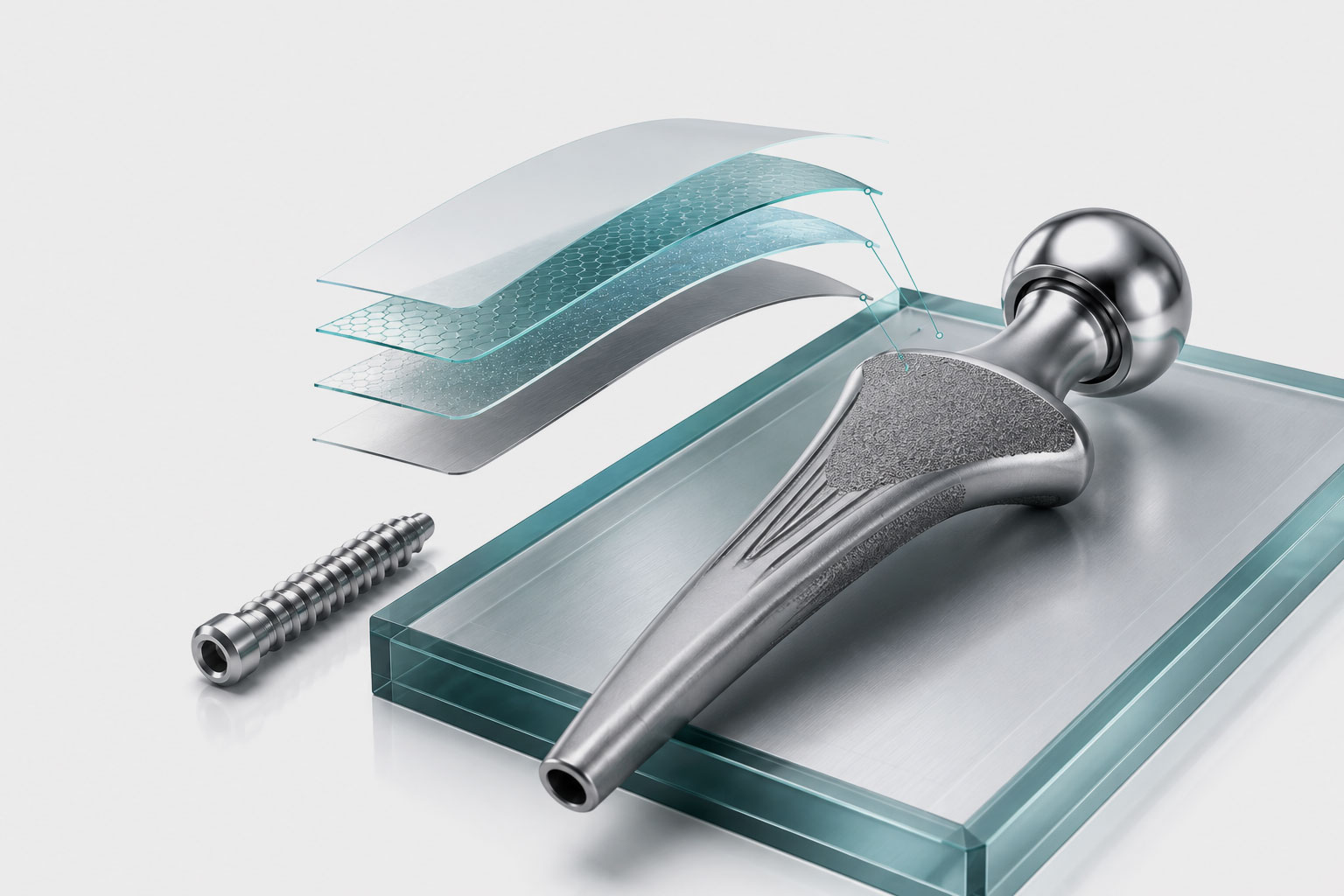
Coatings on implants (screws, joints) that contain micro-porosity can allow bodily fluid ingress, leading to corrosion of the underlying metal and potential ion release.
Interfacial adhesion under physiological load
The bond between biofunctional films (such as antimicrobial silver) and substrates (ceramic, steel, polymer) needs to withstand long-term mechanical and physiological load without delaminating.
PVD SOLUTIONS
Hard wear-resistant coatings (TiN / DLC)
Magnetron sputtering is used to apply dense titanium nitride or diamond-like carbon coatings, intended to extend tool life and edge retention on precision surgical instruments.
Dense, low-porosity coating structure
Ion bombardment and bias control are applied to reduce columnar grain growth, producing a denser film structure intended to limit fluid-penetration pathways.
Pre-clean process for coating adhesion
High-density pre-clean plasma is used prior to coating to promote adhesion, with films validated to the 5B cross-hatch standard under dynamic load conditions.

Discuss Your Process Requirements

Areesys develops PVD platforms for pilot-line development and volume manufacturing, including large-panel advanced packaging, high-aspect-ratio via metallization, display electrodes, precision thin films, and roll-to-roll coating processes.

Share your process specifications and our engineering team can advise on equipment configuration and expected performance.