
![<subject>[background image] image of robotics lab (for a robotics and automation)</subject>](images/HP-B.jpg)
Founded in Silicon Valley, Areesys delivers high-throughput Pilot and Volume Production PVD Platforms tailored for pan-semiconductor, advanced packaging, and emerging energy applications.
Our products and solutions are critical to customers who are at the forefront of next-generation clean energy, displays, and advanced packaging, wafer-level, panel-level, or large-sized substrates.
Our core strength is high-throughput wafer- or panel-level packaging, including High-Density Plasma PVD (HDP-PVD) and high-aspect-ratio TGV (Through Glass Via) applications.
Five industries, one deposition platform.
Where a film has to be thick, uniform, and reach the bottom of a via — our PVD platforms cover wafers, panels, and continuous web, from pilot lines through volume production.
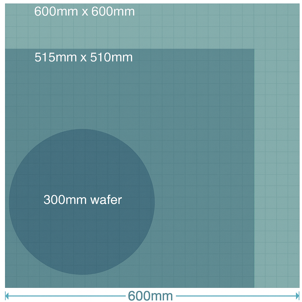
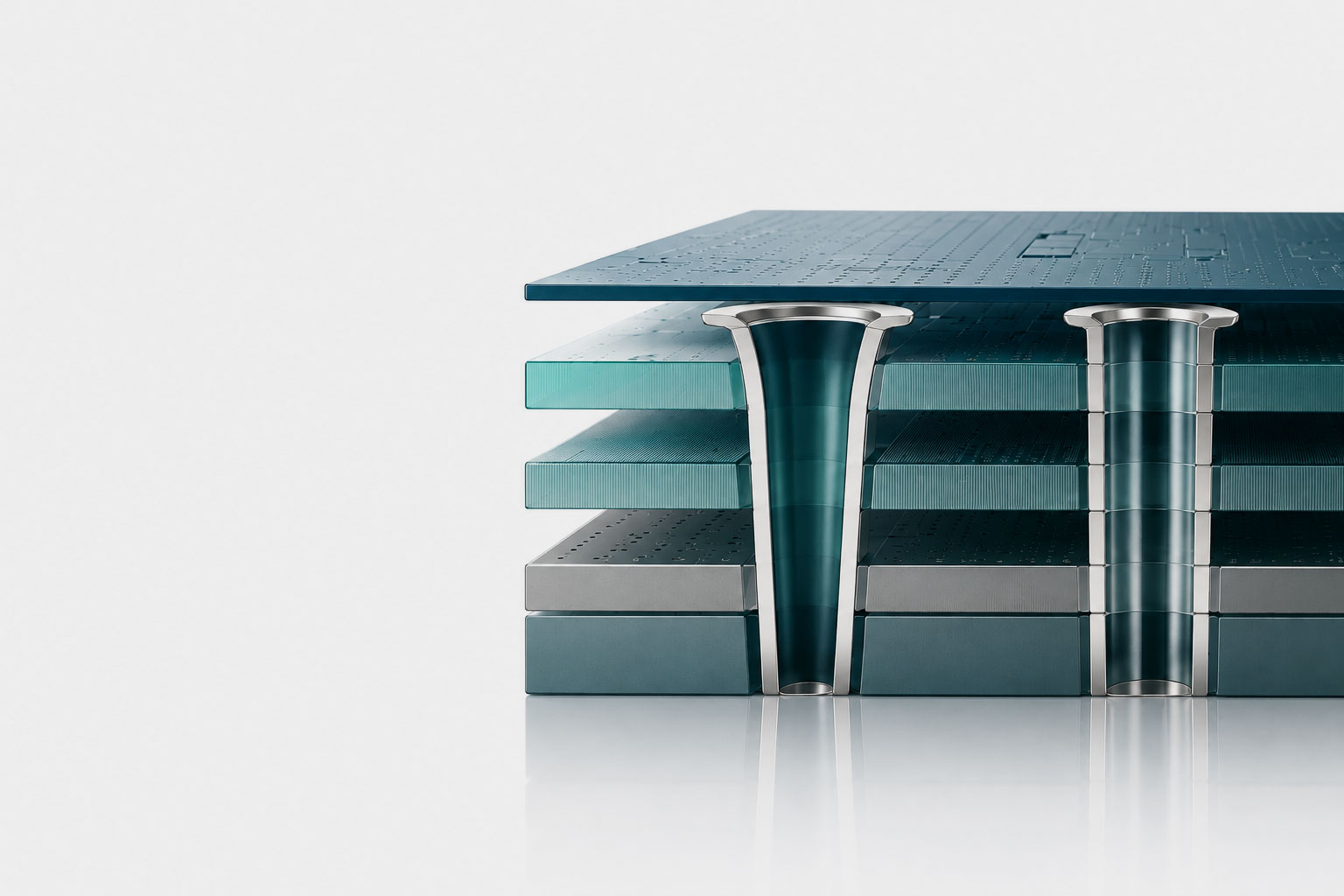
Continuous Ti/Cu seed layers reaching the bottom of deep glass and silicon vias, with panel warpage held in check at 510 × 515 mm.
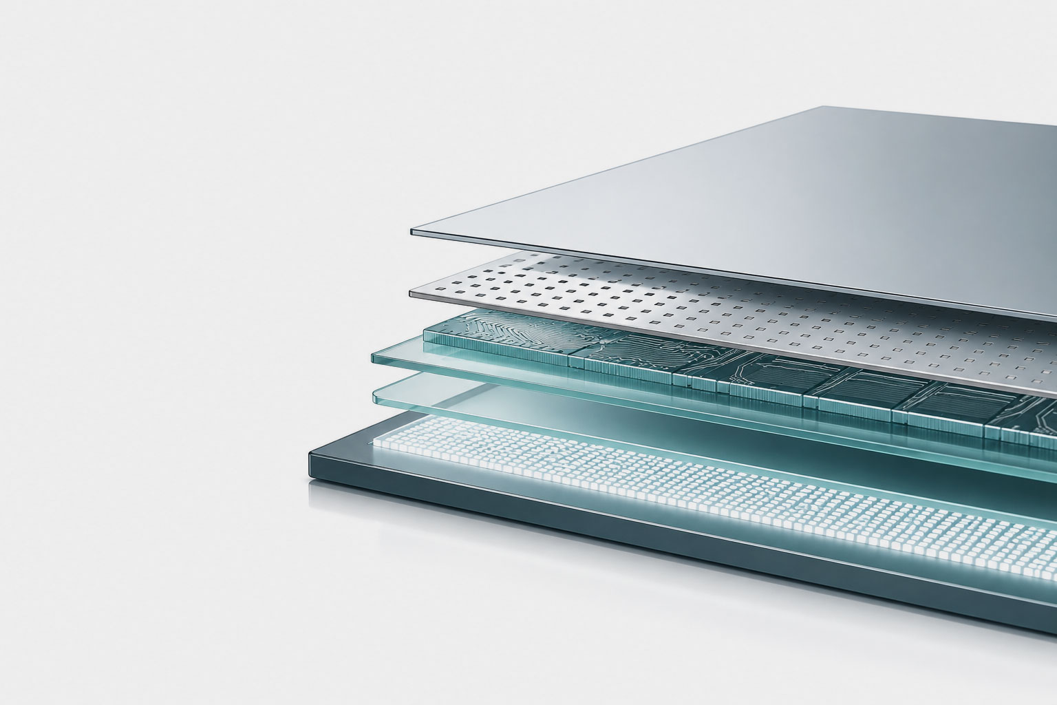
Hundreds of nanometers of Al, Cu, or Mo laid across Gen 6 panels without trading away sheet-resistance uniformity or emitter lifetime.
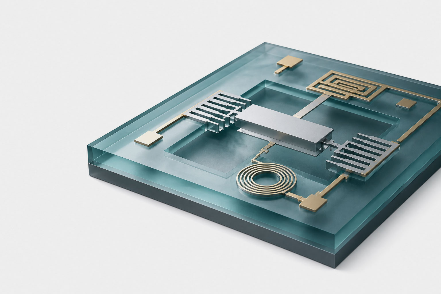
Oriented AlN growth and nanoscale alloy stacks for BAW/SAW filters, acoustic sensors, and magnetic memory devices.
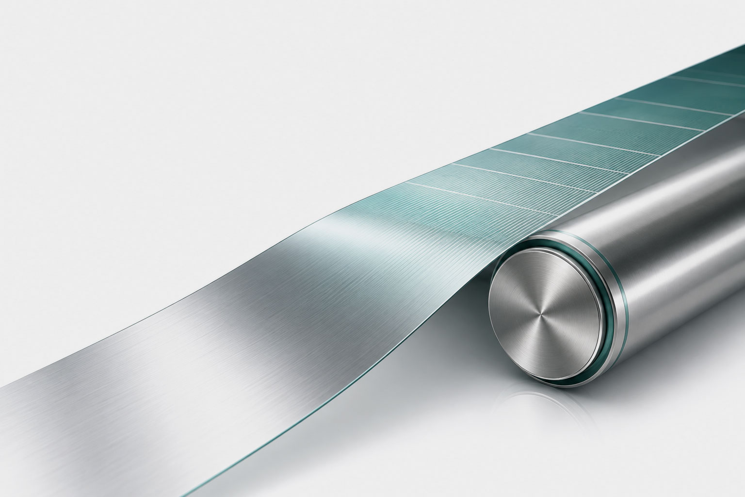
Dry metallization of solar back electrodes and battery current collectors — high target utilization, no plating wastewater.
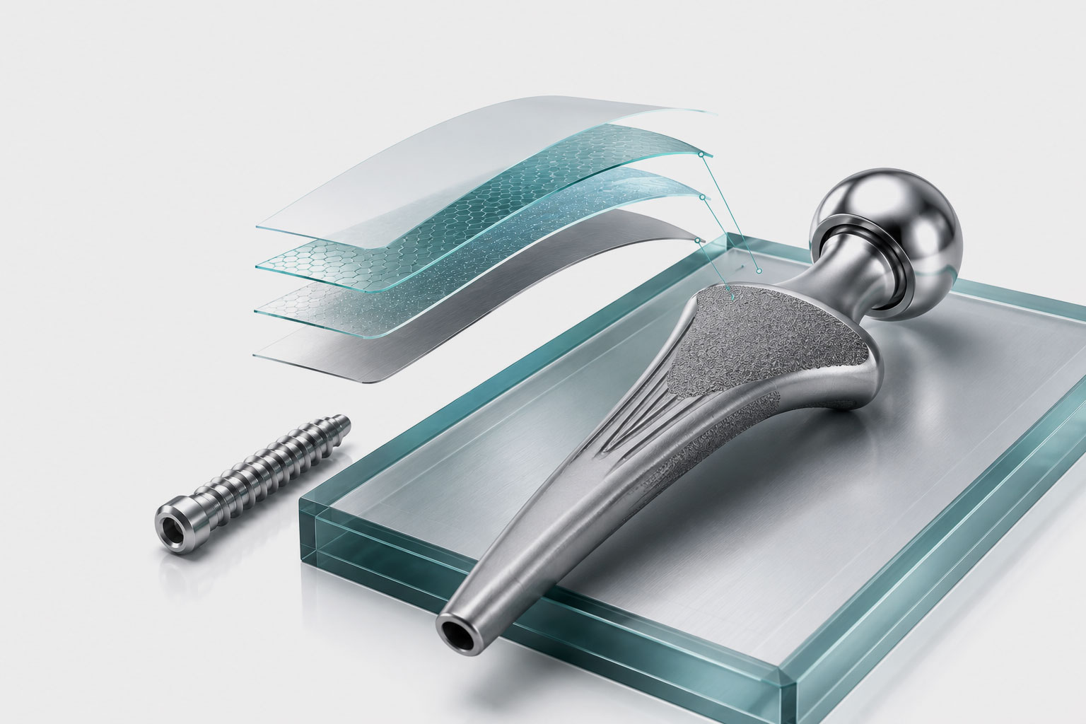
Hard, dense, well-adhered surfaces on titanium implants and instruments, engineered for long-term physiological exposure.
Six fab systems for wafer- and panel-level packaging — sputtering, descum, TGV and TSV metallization — alongside four lab platforms for PLD, magnetron sputtering, e-beam evaporation, and in-situ vacuum clustering.
Explore Fab & Lab Tools

Since 2012, the Silicon Valley based Areesys is in the business to develop advanced manufacturing technologies for the global markets in pan semiconductor, electronics, sensor, flat panel display, renewable energy and energy storage.
Our diversified talents come from a broad industry background. It covers new materials discovery, semiconductor, optoelectronics, energy storage, defense systems, and factory automation. It is our invaluable people who have shaped Areesys’s competitive edge to answer the challenges presented by our customers. As a forward-looking team, we have the right expertise and courage to help our customers, in response to their ever changing needs today and tomorrow.
Let our PVD expers help your company grow
We look forward hearing from you
info@areesys.com690 Saratoga Ave, Ste 100
San Jose, CA 95129,USA
2F-3m No.99, Jingke S. Rd. Nantun Dist.,
Taichung Citiy 408018, Taiwan